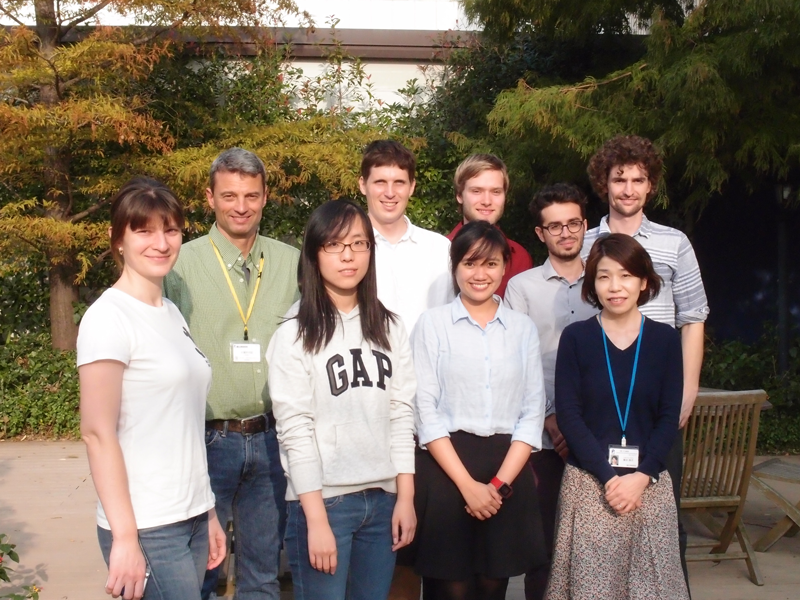
Urs Frey (white shirt, center back row) and his team in the garden area at the RIKEN facilities on Kobe Port Island. Co-authors Alexandra Dudina, Andreas Hierlemann (first and second from left), and first author Florent Seichepine (far right).
Topics:
Topics:
Carbon nanotubes are a hot topic in electronics and other material sciences. But would you believe they might be storming into the fields of biotechnology and medical sciences? Recently I sat down with Urs Frey to discuss this possibility and his recent success in developing a new process for fabricating carbon nanotubes.
How would you simply and briefly express the main findings of your recent study?
Due to its high surface-to-volume ratio and unique electronic properties, carbon nanotubes (CNTs) are a nanomaterial that has the potential to be very good at sensing tiny chemical and biological species. When CNTs are integrated into electronic systems on a large scale, we can achieve highly sensitive, label-free electrical detection. However, this type of integration is still very challenging because of inherent material properties and limitations of the industrial processes used to fabricate standard electronic systems.
To overcome this limitation, we developed a reliable fabrication process that deposits CNTs into a CMOS microsystem. We then performed a simple experiment showing the liquid potential and pH dependency of the sensors, thus demonstrating their applicability for detecting biological processes such as DNA hybridization, molecule detection, and changes in protein shapes.
What is a CMOS system and why is it important?
CMOS stands for “complementary metal–oxide–semiconductor”, and is the most common technology used for making integrated circuits such as microprocessors, computer memories, image sensors, and data convertors. CMOS technology allows complex electronic functions to be integrated into very small pieces of silicon, and when used in a sensor system such as a the light sensor in a digital camera, CMOS allows signals to be amplified and multiplexed right at the source. This keeps noise interference at a minimum and also allows thousands or even millions of sensing elements to be integrated in a very small area. In the context of our work, CMOS was critical for achieving a highly-multiplexed sensing platform with 1024 sensors, and for amplifying and transmitting the minute electrical signals from the CNTs to personal computers for further analysis.
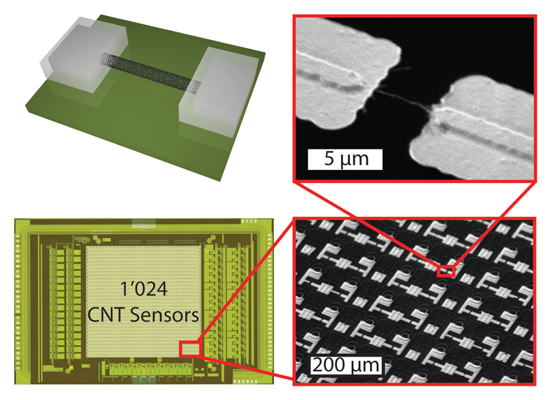
(top left) Illustration of a single CNT sensor. (bottom left) Micrograph of the CMOS system with the CNT sensors in the center. (bottom right) Scanning electron micrograph of the CNT sensor array. The sensor pattern can be seen at medium magnification (200 µm scale bar). (top right) At higher magnification, the two levels of Pt can be seen, and a CNT bundle between the electrodes becomes visible (5 µm scale bar, compare to the illustration on the left).
What are carbon-nanotube sensors and why are they important?
Since carbon nanotubes were first discovered by Professor Sumio Iijima, they have been studied for their outstanding mechanical and electronic properties. Their inert nature and high surface-to-volume ratio render them an ideal material for detecting biological molecules. Recently, CNTs have been used as sensors to detect single molecules of DNA and even changes in the conformation of proteins attached to the surface of DNA. Additionally, by adding specific receptors, such as antibodies or single strained DNA to their surfaces, CNTs can become “functionalized” into sensors that detect specific biomolecules at very low concentrations. This allows the real-time detection of molecules at very low concentrations without the need for target-molecule amplification or fluorescent labelling.
What implications do your findings have?
While several studies have demonstrated that CNTs are outstanding at sensing biological species, using their properties in more widespread applications has proved difficult. Unfortunately, the high sensitivity of CNT sensors also means that baseline fluctuations due to unspecific and random adsorption events are fairly high. This leads to detection errors. Additionally, the limited adsorption area of single-CNT nanosensors leads to slow response times for low concentrations.
In theory, both these limitations can be tackled by integrating large arrays of individual sensor elements. This increases the total absorption area and allows reliable information to be extracted through statistical analysis.
Our work demonstrated that large-scale and reliable integration of CNT sensors is indeed possible. Our new fabrication process can be used for the next type of devices, with applications in point-of-care diagnostics—being able to diagnose a patient on the spot, without the need to send material off to a laboratory for analysis.
How do your findings fit into the larger picture?
Well, over the past decade, the development of new bioelectronics and biosensors based on CMOS technology in many groups around the world (including ours) has enabled the study of neural networks at a completely new scale. Minute electric signals from axonal processes can now be tracked to see how they propagate from one neuron to the next. Now, with the emerging of new platforms integrating nanomaterials to probe chemical species, studying chemical signaling of complex biological systems will soon be possible. In systems such as cultured neuronal networks, our technology may allow chemical communication via neurotransmitters to be recorded at the molecular level.
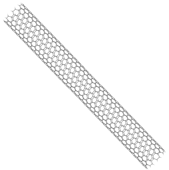
Drawing of a carbon nanotube. Image by User:Gmdm (Wikipedia commons) [GFDL or CC-BY-SA-3.0], via Wikimedia Commons
One of the main challenges of this project was developing a new technology for fabricating nano-sized sensors without the fabrication capabilities of a big, commercial CMOS foundry. Choosing to manipulate particles using an electric field gradient—a process called dielectrophoresis—turned out to be rewarding as we managed to optimize the process and were able to achieve an unexpectedly high yield of functional devices. Of course, none of this would have been possible without an open mind for coping with fabrication limitations and the well-equipped micro-fabrication facilities at RIKEN QBiC and keeping.
What does the future hold for this project?
We are moving forward into two main directions. First, we are working on the complex biochemistry necessary for functionalizing the surface of CNT sensors. This is needed for conducting large-scale sensing applications. Second, we are developing a more versatile CMOS system. Greater versatility will allow more direct, real-time control of large-scale CNT integration, while at the same time increase the sensor density, integrating 10,000 individually addressable CNT sensors on a single device.
What else can you say about this project?
Developing this project at RIKEN QBiC has been challenging for our team. The successful outcome shows that the proximity of scientists from different fields can really be a catalyst that brings new ideas and concepts to existing questions and problems. We hope that our technology will inspire other groups to develop a new generation of biosensors with applications in basic research and in early point-of-care diagnostics.
Until recently Frey was the leader of the Frey Initiative Research Unit at RIKEN QBiC in Kobe, Japan. Currently, he is at the Department of Biosystems Science and Engineering at ETH Zurich in Basel, Switzerland and together with the Spin-off company MaxWell Biosystems, he is commercializing CMOS-based bioelectronics systems. ?
[vifblike]
Carbon nanotubes are a hot topic in electronics and other material sciences. But would you believe they might be storming into the fields of biotechnology and medical sciences? Recently I sat down with Urs Frey to discuss this possibility and his recent success in developing a new process for fabricating carbon nanotubes.
How would you simply and briefly express the main findings of your recent study?
Due to its high surface-to-volume ratio and unique electronic properties, carbon nanotubes (CNTs) are a nanomaterial that has the potential to be very good at sensing tiny chemical and biological species. When CNTs are integrated into electronic systems on a large scale, we can achieve highly sensitive, label-free electrical detection. However, this type of integration is still very challenging because of inherent material properties and limitations of the industrial processes used to fabricate standard electronic systems.
To overcome this limitation, we developed a reliable fabrication process that deposits CNTs into a CMOS microsystem. We then performed a simple experiment showing the liquid potential and pH dependency of the sensors, thus demonstrating their applicability for detecting biological processes such as DNA hybridization, molecule detection, and changes in protein shapes.
What is a CMOS system and why is it important?
CMOS stands for “complementary metal–oxide–semiconductor”, and is the most common technology used for making integrated circuits such as microprocessors, computer memories, image sensors, and data convertors. CMOS technology allows complex electronic functions to be integrated into very small pieces of silicon, and when used in a sensor system such as a the light sensor in a digital camera, CMOS allows signals to be amplified and multiplexed right at the source. This keeps noise interference at a minimum and also allows thousands or even millions of sensing elements to be integrated in a very small area. In the context of our work, CMOS was critical for achieving a highly-multiplexed sensing platform with 1024 sensors, and for amplifying and transmitting the minute electrical signals from the CNTs to personal computers for further analysis.
(top left) Illustration of a single CNT sensor. (bottom left) Micrograph of the CMOS system with the CNT sensors in the center. (bottom right) Scanning electron micrograph of the CNT sensor array. The sensor pattern can be seen at medium magnification (200 µm scale bar). (top right) At higher magnification, the two levels of Pt can be seen, and a CNT bundle between the electrodes becomes visible (5 µm scale bar, compare to the illustration on the left).
What are carbon-nanotube sensors and why are they important?
Since carbon nanotubes were first discovered by Professor Sumio Iijima, they have been studied for their outstanding mechanical and electronic properties. Their inert nature and high surface-to-volume ratio render them an ideal material for detecting biological molecules. Recently, CNTs have been used as sensors to detect single molecules of DNA and even changes in the conformation of proteins attached to the surface of DNA. Additionally, by adding specific receptors, such as antibodies or single strained DNA to their surfaces, CNTs can become “functionalized” into sensors that detect specific biomolecules at very low concentrations. This allows the real-time detection of molecules at very low concentrations without the need for target-molecule amplification or fluorescent labelling.
What implications do your findings have?
While several studies have demonstrated that CNTs are outstanding at sensing biological species, using their properties in more widespread applications has proved difficult. Unfortunately, the high sensitivity of CNT sensors also means that baseline fluctuations due to unspecific and random adsorption events are fairly high. This leads to detection errors. Additionally, the limited adsorption area of single-CNT nanosensors leads to slow response times for low concentrations.
In theory, both these limitations can be tackled by integrating large arrays of individual sensor elements. This increases the total absorption area and allows reliable information to be extracted through statistical analysis.
Our work demonstrated that large-scale and reliable integration of CNT sensors is indeed possible. Our new fabrication process can be used for the next type of devices, with applications in point-of-care diagnostics—being able to diagnose a patient on the spot, without the need to send material off to a laboratory for analysis.
How do your findings fit into the larger picture?
Well, over the past decade, the development of new bioelectronics and biosensors based on CMOS technology in many groups around the world (including ours) has enabled the study of neural networks at a completely new scale. Minute electric signals from axonal processes can now be tracked to see how they propagate from one neuron to the next. Now, with the emerging of new platforms integrating nanomaterials to probe chemical species, studying chemical signaling of complex biological systems will soon be possible. In systems such as cultured neuronal networks, our technology may allow chemical communication via neurotransmitters to be recorded at the molecular level.
Drawing of a carbon nanotube. Image by User:Gmdm (Wikipedia commons) [GFDL or CC-BY-SA-3.0], via Wikimedia Commons
One of the main challenges of this project was developing a new technology for fabricating nano-sized sensors without the fabrication capabilities of a big, commercial CMOS foundry. Choosing to manipulate particles using an electric field gradient—a process called dielectrophoresis—turned out to be rewarding as we managed to optimize the process and were able to achieve an unexpectedly high yield of functional devices. Of course, none of this would have been possible without an open mind for coping with fabrication limitations and the well-equipped micro-fabrication facilities at RIKEN QBiC and keeping.
What does the future hold for this project?
We are moving forward into two main directions. First, we are working on the complex biochemistry necessary for functionalizing the surface of CNT sensors. This is needed for conducting large-scale sensing applications. Second, we are developing a more versatile CMOS system. Greater versatility will allow more direct, real-time control of large-scale CNT integration, while at the same time increase the sensor density, integrating 10,000 individually addressable CNT sensors on a single device.
What else can you say about this project?
Developing this project at RIKEN QBiC has been challenging for our team. The successful outcome shows that the proximity of scientists from different fields can really be a catalyst that brings new ideas and concepts to existing questions and problems. We hope that our technology will inspire other groups to develop a new generation of biosensors with applications in basic research and in early point-of-care diagnostics.
Until recently Frey was the leader of the Frey Initiative Research Unit at RIKEN QBiC in Kobe, Japan. Currently, he is at the Department of Biosystems Science and Engineering at ETH Zurich in Basel, Switzerland and together with the Spin-off company MaxWell Biosystems, he is commercializing CMOS-based bioelectronics systems. ?
[vifblike]
Further reading:
kylius wilkins
Kylius is the English Language Science Communicator for RIKEN QBiC in Suita, Osaka
I’m trained as a veterinarian but I love talking to particle physicists! When I’m not working, I like to watch my two boys play baseball, walk in the woods, eat raw fish, and soak in onsens.
[yuzo_related]


